
Optimizing the power consumption of the FT-817 when operating on battery power
|
Current consumption of the FT-817 is both modest and moderate:
While it consumes (by far) less current than the average HF it does
consume
a fair amount of current as compared with a portable rig such as an
HT.
Another thing that should be considered is power
consumption:
As noted by the chart to the right (which is similar -
but
not identical to that on the FT-817 Current
Consumption
page) the current consumption rises only slightly with increased supply
voltage, but since power is the product of voltage and
current,
the power consumption rises dramatically with voltage. This is
because
the '817 uses linear voltage regulation for the radio's
internal
circuitry. While switching supplies would result in better
efficiency,
it would be "risky" (and somewhat expensive) to place a switching
supply
(which is, in effect, a high-powered oscillator) circuit amongst
sensitive
RF circuits within the radio without causing RFI problems.
|
Voltage |
(mA) |
(watts) |
| 7.5 | 273 | 2.05 |
| 8.0 | 274 | 2.12 |
| 8.5 | 276 | 2.35 |
| 9.0 | 276 | 2.48 |
| 10.0 | 279 | 2.79 |
| 11.0 | 281 | 3.09 |
| 12.0 | 284 | 3.41 |
| 13.0 | 287 | 3.73 |
| 14.0 | 291 | 4.07 |
| 15.0 | 294 | 4.41 |
| 16.0 | 297 | 4.75 |
The chart reveals that the most efficient operation may be obtained by operating the receiver at the lowest voltage. In real life, efficiently adjusting battery voltage is not practical: If you are running from a 12 volt Lead-Acid, NiCd or NiMH battery pack, you will get 12 volts (more or less) out of the battery pack pretty much throughout the discharge life of the pack. You could adjust the tap of the battery pack to provide the 8 volts (or so) that would reduce power consumption - but you'd then be discharging the cells in the pack unevenly - a literal death sentence for a series-connected NiCd pack (and it isn't very good for other types of packs either!)
What you need is the DC equivalent of a transformer. The ideal transformer is capable of taking a higher AC voltage and lower current and transforming it to a lower voltage and higher current: The power input and output are going to be the same for the ideal transformer (i.e. converting 100 volts at 1 amp - which is 100 watts - gets converted, say, to 1 volt and 100 amps - also 100 watts.) Obviously, you aren't going to get AC directly from the batteries.
Reducing power consumption:
Fortunately, technology has the answer: A switching supply.
It was just mentioned that such a supply can be somewhat expensive
(I
guess it all depends on what you consider to be expensive and how much
you value increased battery operating time when in the middle of
nowhere...)
and prone to cause QRM to the receiver - but the latter point can be
mitigated
with proper design and shielding.
|
Voltage |
Current (mA) |
Current (mA) |
Power (watts) |
% |
| 9.75 | 31.3 | 270 | 2.63 | 86 |
| 10.0 | 34.1 | 265 | 2.64 | 86 |
| 10.25 | 35.4 | 260 | 2.70 | 84 |
| 10.5 | 36.8 | 256 | 2.70 | 84 |
| 11.0 | 39.5 | 249 | 2.74 | 83 |
| 11.5 | 42.0 | 243 | 2.79 | 81 |
| 12.0 | 44.4 | 237 | 2.84 | 80 |
| 13.0 | 48.8 | 227 | 2.95 | 77 |
| 14.0 | 52.7 | 218 | 3.05 | 74 |
| 15.0 | 56.0 | 210 | 3.15 | 72 |
| 16.0 | 58.7 | 203 | 3.25 | 70 |
| 17.0 | 61.0 | 197 | 3.35 | 68 |
The table to the left shows the result of using the described switching supply with the '817 (more on this supply later...) and its current/power consumption and efficiency versus voltage. Most switching supplies operate at less than their ultimate efficiency when lightly loaded, so I configured the '817 to consume reduced current (i.e. front antenna relay, backlight off, minimum volume, and set to FM) to show a "worst case" scenario. Also, the switching supply is set to output 8.25 volts - a reasonable "minimum" voltage that still allows a minimum of receiver performance degradation - which minimizes current consumption.
As you can see, the '817 itself is consuming 275 milliamps - which correlates to a power consumption of 2.27 watts. The minimum switching supply input voltage is 9.75 volts: Operating at a voltage lower than this causes the switching regulator to shut down (it was designed for a nominal 12 volt input.)
Note that even at the lowest input voltage (9.75 volts) the current consumption of the switching supply running the '817 is already below that of the '817 (running at 8.25 volts - the output voltage of the switcher) in spite of the switching supply inefficiency. What's more, if you were to operate the '817 at 9.75 volts directly (using the same configuration) it would consume about 280 milliamps - a power consumption of 2.73 watts - which is less that then switching supply consumes when the radio is operated at the same voltage. In fact, you'll note that even with the switching regulator's losses, the combination consumes less current and less power than the '817 by itself. (Is that an awkward paragraph, or what?)
Reducing power consumption during transmit:
As in the case of receive, the power consumption also increases with
power supply voltage during transmit. This is spelled out in K6XX's
FT-817 page (specifically, the Current
consumption at 5 watts output graph) as well as the chart below and
to the right. At the highest power setting (nominally 5 watts)
the
current consumption is 1.9-2.0 amps across the voltage operating
range. In reality, the '817 will not put out a full 5 watts at
the
low end of the voltage range (8-10 volts) on all bands, but by the time
you get up to 11 volts, the full output power is pretty much available,
so it really doesn't make much sense to increase operating voltage
further.
|
Voltage |
Current (Amps) |
Power (watts) |
% |
Input Current |
Input Power |
|
| 11.25 | 2.1 | 23.6 | 91 | 1.97 | 22.28 | |
| 11.5 | 2.0 | 23.0 | 94 | 1.97 | 22.66 | |
| 12.0 | 1.95 | 23.4 | 92 | 1.96 | 23.52 | |
| 12.5 | 1.83 | 22.9 | 94 | 1.96 | 24.50 | |
| 13.0 | 1.75 | 22.75 | 95 | 1.95 | 25.35 | |
| 13.5 | 1.7 | 22.95 | 94 | 1.95 | 26.33 | |
| 14.0 | 1.65 | 23.1 | 93 | 1.92 | 26.88 | |
| 15.0 | 1.55 | 23.25 | 93 | 1.90 | 28.50 | |
| 16.0 | 1.45 | 23.2 | 93 | 1.89 | 30.24 | |
| 17.0 | 1.35 | 22.95 | 94 | Don't! | (n/a) |
The switching supply is designed such that when transmitting, it can increase its output voltage from 8.25 to approximately 11 volts (10.93 volts, actually...) to allow for a full 5 watts output on all bands. If you are not using the high power setting the radio operates just fine with the lower 8.25 volts - and with increased efficiency. From the chart, you can see that at voltages equal to and above 12 volts, efficiency is gained in spite of the losses of the switching regulator, as compared to running the '817 directly from the same voltage.
Introducing the
"buck"
type switching regulator:
 |
How does the inductor help things? The nature of an inductor is to resist a change in the flow of current. This means that even if Vout is shorted out, at the instant that the switch is closed, no current flows. After a short while, energy builds up in Ls (in the form of a magnetic field) and current starts to flow, eventually reaching saturation of the inductor - a state at which no more energy may be stored.
The instant that the switch is opened , the current flow disappears and the magnetic field begins to collapse and a negative voltage appears at the junction of the switch and the diode. Were the diode not present, that voltage could (theoretically) rise to infinity - but the diode clamps this voltage at either 0.6 volts (for a standard silicon diode) or about 0.2 volts (for a schottky diode.) With the "switch" end of the diode "clamped" near ground, the energy from the inductor dumps into Cfilt as a positive voltage. Since the amount of energy stored in Ls is somewhat proportional to the length of time the switch is closed, the amount of energy output from this buck regulator can be controlled by how often and for how long the switch is closed.
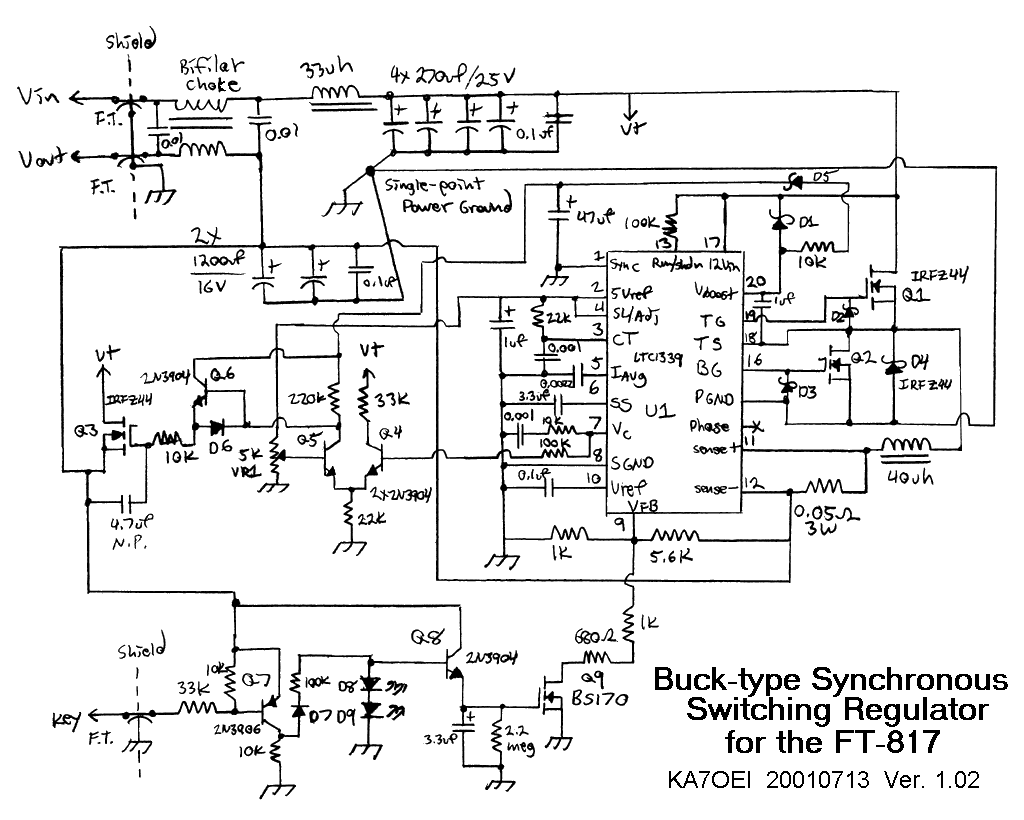
A Switching Regulator for the FT-817:
Because the described circuit is a "one-off" unit, it was built using perfboard and no printed circuit board was designed.
The schematic of the switching regulator may be found here. This is a scan of a hand-drawn schematic. At some point, I'll render it in a purely electronic format. Note that it should be printed in landscape mode. Its resolution may necessitate saving to disk and printing from another program.
Schematic Errata:
An explanation of the circuit:
Before I go any further, let me explain that while I believe this diagram to be correct, it may contain errors that I have not (yet) noticed, so there are no warranties expressed or implied. Also, there are a few modifications/changes that will be made in the future.
The heart of the switcher is U1, a Linear Technologies LT1339 High Power DC/DC Synchronous Switching Controller. What this means (in plain speak) is that this chip can be used to make all sorts of switching supplies and in this case, this versatile chip is being used as a buck-type switching controller.
 |
Because this chip has no on-board high-power switches of its own, outboard MOSFET switches are used. This chip has onboard voltage references and regulators, as well as the necessary logic to perform synchronous switching. What does "synchronous" mean in this context? Remember in the diagram above that there is a diode to ground on the "switch" side of the inductor. The diode will (because we 'canna change the laws of physics!) have a voltage drop associated with it - and a voltage drop means that there will be some loss in efficiency. Replacing that diode with a MOSFET (that we can turn on like a switch in a manner that is synchronized and opened when the other switch is closed to prevent shorting the Batt+ to ground - hence the term "synchronous") can reduce this "diode voltage drop" to a value commensurate with the "ON" resistance of the MOSFET - a resistance that can be in the thousandths of ohms if the appropriate MOSFET is chosen and the current through it. This technique can raise the efficiency by between 5 and 10 percent. The MOSFETs used are IRFZ44N's and these devices are rated for 55 volts, a drain current of 41 amps and an "on" resistance of 0.024 ohms.
MOSFET Q1 is used as the "Switch" while Q2 is used as the replacement for the "diode". Additional diodes (i.e. D1-D4) are placed around the MOSFETs to provide protection to the devices as well as "catch" transients that the transistors may miss before they are turned on by U1. The 40 microhenry inductor stores energy when Q1 is turned on and a pair of low-inductance (extremely important for "clean" operation of a switching supply) 1200 uF capacitors provide output filtering. U1 has an on-board voltage booster that develops over 20 volts to allow the use of inexpensive low-resistance N-channel MOSFETS (which are more readily available than similar P-channel devices.) It also contains current sensing circuitry which can be used to limit output current to a preset value of 2.5 amps - determined in this case by the 0.05 ohm resistor.
The output voltage is divided (using resistors) and applied to pin 9 (Vfb) to set the voltage to the specified value. Normally, the divider consisting of the 1k and 5.6k resistors sets the output to 8.25 volts - a voltage that can efficiently run the receiver with little operational degradation as well as the transmitter at lower power. For transmitting at high power, the KEY input can be grounded (by using the TX GND pin on the FT-817's ACC jack) which turns on Q7, Q8, and then Q9. LEDs D8 and D9 form a sort of "Zener" diode - limiting the voltage to about 4 volts. Q8 acts as an emitter follower, quickly charging the 3.3 microfarad capacitor when the transmitter is keyed, thus turning on Q9. This adds the "seriesed" 1k and 680 ohm resistors in parallel with the 1k Vfb resistor, causing the regulator's output voltage to increase to about 11 volts. When the radio is unkeyed, the 3.3uf capacitor is discharged slowly, allowing the output voltage of the regulator to slowly return to 8.25 volts again. Note that this "slow" return to the 8.25 volt level is necessary as it prevents the voltage from bouncing wildly during quick transmit/receive transitions (such as during CW operation) and (more importantly) it keeps U1 from briefly shutting down if the voltage reference decreases suddenly, as it is wont to do.
Any "dropping" voltage regulator (that is, any regulator that takes a higher voltage down to a lower one) has a dropout voltage - that is, the minimum difference between the input and output voltage required to keep the output in regulation. In the case of the LT1339 in this configuration, this voltage is about 1.75 volts under full (2 amp) load. The values of the resistor and capacitor at pin 3 have been selected to minimize this voltage (but setting a very high maximum duty cycle) but it was still desired that a lower dropout voltage be possible. Just using the switching regulator alone the "dropout" would have meant that operation with input voltages below 10.5 to 11 volts would have been compromised.
The answer to this problem is to "wrap" a linear regulator around the switching regulator.
Pin 7 is part of the voltage regulation circuit, providing "compensation" to keep the output voltage from oscillating under certain conditions. It can also be used to detect when the regulator is no longer able to maintain the desired output voltage - a condition that can be detected when the output at this pin goes above (in this case) 3.25 volts.
Potentiometer VR1 is (carefully) set to provide a threshold comparison voltage: When the output of pin 7 goes above this voltage the pair is unbalanced and Q5 stops conducting. The collector of Q5 is pulled up to about 20 volts (because some voltage is "stolen" from U1's boost supply) which drives Q6, an emitter follower. This voltage then turns on Q3 which essentially connects the input to the output enough to maintain the voltage. The result? The dropout voltage is reduced to approximately 0.3 volts. Because the input/output voltage differential is so low under these conditions, relatively little energy is lost due to the linear regulation.
Some of the most important features of this (and
almost
any) switching regulator is the single-point ground, filtering and
shielding.
As seen from the schematic, the high-current points are all tied
together
at one common point - using heavy gauge wire. Also, as the
picture
at the top of the page shows, this circuit is packaged in a die-cast
aluminum
box. Furthermore, feedthrough capacitors are used to further
reduce
the conduction of RF energy from the switching supply. Finally,
the
input/output power leads pass through a bifilar inductor to increase
the
reactance of high frequency components before they get
to
the feedthrough capacitors. The result of all of this? On
160
meters, the harmonics (the switching supply operates at approximately
100
kHz) are weakly audible only if the FT-817's antenna is
connected
directly to either the input or output terminals via a
0.1
uF capacitor, and are inaudible on the higher amateur bands.
Needless
to say, they are not audible at all under normal operation because one
doesn't normally connect one's antenna to the power supply.
Again, one of the more important aspects of component selection of
this (or other) switching regulator circuits is the proper use of the
electrolytic filter capacitors. For reliability and good
efficiency, one MUST use low ESR
electrolytics: Ordinary, standard electrolytic capacitors will
not
work in this application! Why? At the switching
frequencies involved (around 100 kHz) the internal resistance of
"ordinary" electrolytic capacitors isn't as low as you might think a
1000uF capacitor at 100 kHz might be! Because several amps
may be flowing through the capacitor during the switching cycle, even
low amounts of resistance will produce heat - which means loss of
efficiency, which means poor reliability! In other words, if the
capacitors get warm, they are either bad, or the wrong types!
Pretty much all low-ESR electrolytics have a
temperature rating of 105C (as opposed to 85C) - but not all 105C
capacitors are low-ESR types! The special low ESR types are
especially designed for use in switching supplies and, in many cases,
several units are paralleled to distribute the "ripple" current through
several capacitors: This is why one might see three 470uF
capacitors in parallel on a switching power supply instead of a single
1500uF capacitor!
If you do use a "standard" capacitors, you can expect several things:
Possible future enhancements:
 |
How is this connected to the radio?
There are two ways to connect this switching supply to the FT-817: Via the back panel, or through the battery connector. The rear panel connector has the advantage that it is easily accessible. The disadvantage is that the "Auto" mode (where the panel backlight shuts off automatically) doesn't function. The battery connector has the advantage that the "Auto" mode does work, but the disadvantage is that it is awkward to connect to the radio (the connectors are a bit difficult to come by and are awkward to connectorize without the proper tools.) Taking the more difficult path, I chose the latter option.
The "battery connector adapter" is built using a piece of glass
epoxy
circuit board (with the copper removed and painted with black epoxy
paint)
but one could use the battery cover from the '817 (or you could order a
replacement.) The "fingers" consist of small pieces of
glass-epoxy
board epoxied in place, while the latch portion consists of a piece of
Copperweld (tm) wire epoxied into place. A rubber grommet is used
for a strain relief, and the power connection goes through a
bifilar-wound
toroid inductor. Across the output of this inductor goes to 5
paralleled
220 uF capacitors to assure a low-impedance supply, a reverse-biased
diode
(to blow the inline fuse in the event reverse polarity is applied) and
a 0.01 microfarad capacitor across the diode to guarantee low impedance
even at RF.
For more information on use of this circuit with Lithium-Ion cells, visit the Operating the FT-817 from Lithium-Ion (Li-Ion) cells page.
Work continues on
this
page - please revisit soon!
The KA7OEI FT-817 "Front Page" - This is, well, the "front" page of the '817 pages here...
Any comments or questions? Send an email!
This page maintained by Clint Turner, KA7OEI
and
was last updated on 20150415. (Copyright 2001-2015 by Clint
Turner)